
What are the tolerances for PCB prototypes?
tolerances for PCB prototypes
Tolerances for PCB prototypes refer to the allowable variations in the physical dimensions and electrical properties of a printed circuit board during the manufacturing process. These tolerances play a significant role in ensuring the functionality and reliability of the final PCB prototype. When designing a PCB prototype, engineers need to define the acceptable limits for various parameters, such as trace width, hole diameter, component placement, and overall board dimensions, as these factors influence how well the prototype performs in its intended application.
One of the most important tolerances to consider in a pcb prototype is the trace width. The trace width defines the thickness of the copper traces that carry electrical signals and power throughout the PCB. In high-frequency or high-power applications, the trace width must be precise to ensure that the board can handle the electrical load and signal integrity requirements. The tolerance for trace width varies depending on the manufacturing process and the technology used. For standard PCB prototypes, the typical tolerance for trace width can range from ±10% to ±20%. However, for more precise applications, such as RF or high-speed circuits, the tolerance may be tighter, requiring more accurate trace width specifications.
Another critical tolerance is the hole diameter, especially for vias and component leads. In PCB prototypes, vias are used to connect different layers of the board, and components are inserted into holes for electrical connections. The hole diameter must be precisely controlled to accommodate the components’ leads or ensure the via can properly conduct electrical signals between layers. The standard tolerance for hole diameters in a PCB prototype typically ranges from ±0.1mm to ±0.2mm, depending on the board’s complexity and the manufacturer’s capabilities. For smaller components or microvia designs, tighter tolerances are required to ensure proper fit and function.
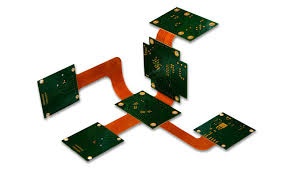
What are the tolerances for PCB prototypes?
Component placement tolerance is also crucial in PCB prototypes. The placement of components, such as resistors, capacitors, and ICs, needs to be highly accurate to ensure the functionality of the final board. Inaccuracy in component placement can lead to issues like short circuits, incorrect signal routing, or poor performance. The tolerance for component placement typically ranges from ±0.1mm to ±0.2mm, depending on the type of component and the technology used. For fine-pitch components or high-density PCBs, tighter tolerances may be required to ensure correct placement and prevent manufacturing defects.
Board dimensions are another area where tolerances are important. The overall dimensions of the PCB prototype, including length, width, and thickness, must be within a specified tolerance to ensure that the board fits properly in the final assembly or housing. The tolerance for PCB dimensions is generally around ±0.2mm to ±0.5mm, but this can vary based on the complexity of the board and the specific requirements of the project. For more complex boards, such as rigid-flex or multi-layer PCBs, tighter tolerances may be needed to maintain the overall integrity and compatibility of the design.
Electrical tolerances are also critical in PCB prototypes, especially in high-precision applications. These tolerances relate to factors such as impedance control, signal integrity, and power distribution. For instance, in high-speed PCBs, maintaining consistent impedance is crucial for signal transmission without distortion. Tolerances for impedance in these cases are typically very tight, often within ±5% to ±10%, depending on the type of PCB and the design requirements.